(China (Mainland))


Product Summary
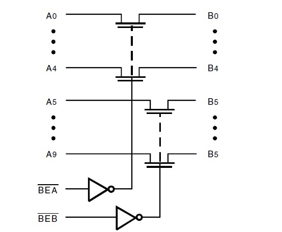
The QS3L384QX is a high-speed CMOS TTL-compatible bus switch. The low ON resistance of the QS3L384QX allows inputs to be connected to outputs without adding propagation delay and without generating additional ground bounce noise. The Bus Enable (BE) signals turn the switches on. Two bus enable signals are provided, one for each of the upper and lower five bits of the two 10-bit buses. The QS3L384QX is characterized for operation at -40℃ to +85℃.
Parametrics
QS3L384QX absolute maximum ratings: (1)VTERM Supply Voltage to Ground: -0.5 to +7 V; (2)VTERM DC Switch Voltage VS: -0.5 to +7 V; (3)VTERM DC Input Voltage VIN: -0.5 to +7 V; (4)VAC AC Input Voltage (pulse width ≤20ns): -3 V; (5)IOUT DC Output Current: 120 mA; (6)PMAX Maximum Power Dissipation (TA = 85℃): 0.5 W; (7)TSTG Storage Temperature: -65 to +150 ℃.
Features
QS3L384QX features: (1)Enhanced N channel FET with no inherent diode to Vcc; (2)5Ω bidirectional switches connect inputs to outputs; (3)Zero propagation delay, zero added ground bounce; (4)Ultra low power with 0.2μA typical Icc; (5)Undershoot clamp diodes on all switch and control inputs; (6)Two enables control five bits each; (7)Available in SOIC, QSOP, and TSSOP packages.
Diagrams
 |
 QS3L384PAG |
Other |
|
Data Sheet |
Negotiable |
|
||||
|
QS3L384PAG8 |
Other |
|
Data Sheet |
Negotiable |
|
||||
|
QS3L384QG |
Other |
|
Data Sheet |
Negotiable |
|
||||
|
QS3L384QG8 |
Other |
|
Data Sheet |
Negotiable |
|
||||